Activity 2.2.3 Nor logic design
Introduction
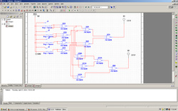
In this activity you will revisit the voting booth monitoring system introduced in Activity 2.2.3 NAND Logic Design. Specifically, you will be implementing the NOR only combinational logic circuits for the two outputs Booth and Alarm. In terms of efficiency and gate/IC utilization, these NOR only designs will be compared with the previously designed AOI and NAND implementations.
Conclusion
1. For your NOR implementations, how many ICs (i.e., 74LS02 chips) were required to implement your circuits? Again, we are counting ICs, not gates.
2 IC chips-booth
3 IC chips-alarm
2. In terms of hardware efficiency, how does the NOR implementation compare to the AOI implementation (Refer to Activity 2.2.3 NAND Logic Design)?
Less efficient for both of them. More wire and more chip.
3. In terms of hardware efficiency, how does the NOR implementation compare to the NAND implementation in Activity 2.2.3 NAND Logic Design?
The NAND implementation is more efficient
NOR gates are available with three inputs (74LS27). Could this chip have been used for this design? If so, how would it have affected the efficiency of the design?
