Project 2.3.2
Introduction
In your digital electronics class of 20, there is a 6.8% probability that two of you share the same date of birth. This is assuming that you are all the same year level (sophomore/junior). If you are not, the probability would be even lower.
Your date of birth makes you unique. We are going to use this uniqueness to design a circuit that will display your date of birth on a single seven-segment display. Admittedly, this design does not have any real practical application, but is a fun exercise that will bring together all of the design techniques that you have learned in this lesson.
Your date of birth may make you unique in your class, but in 2006 there were 263,898,574,096 births world-wide. This means that on a daily basis, over 700,000,000 individuals share the same date of birth.
Conclusion
Using your engineering notebook/portfolio as a guide, write a conclusion (minimum 250 words) that describes the process that you used to design, simulate, and build your Date of Birth circuit. This conclusion must include all of your design work (i.e., truth table, K-Maps, etc), preliminary and final schematics, parts list, and a digital photograph of your final circuit. The documentation should be complete enough that another student with the same knowledge of digital electronics could reproduce your design without any additional assistance.
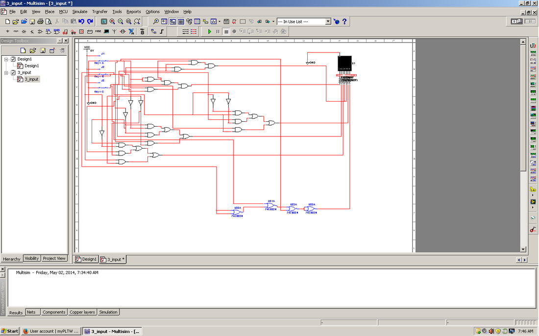
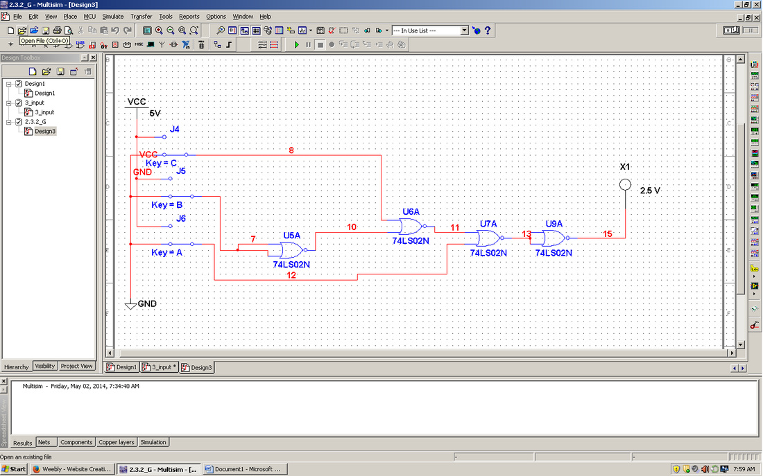
First, I made a truth table to determine which combination of inputs would trigger which output number or hyphen. Then, I created a final truth table to determine which segments of the display would turn on for each combination to get the number or hyphen using Multisim. After that, I created a circuit for each of the segments using the logic converter tool on the right side of the Multisim interface. Two of the segments had to be NAND logic and one had to be NOR logic. The two segments that I used for NAND logic were the A segment and D segment, and the NOR logic was the G segment. Once I had completed each circuit I combined them all into one big circuit while simplifying as much of it as I could. I then printed out the circuit, but it was too big to fit on one page so it ended up on two pages so I had to tape them together. As I bread boarded I crossed out which wires and gates I had already wired on the papers I printed out. That way I could keep track of what was done and what wasn’t done.
While I bread boarded I took special care to ensure I didn’t puncture the metal at the bottom of the bread board. When I finished wiring the circuit I tested it to make sure it was working, but I didn’t have switches so I just used 3 wires and plugged them into the power section for when they were supposed to be on.
To complete the circuit I used one NOR chip, two NAND chips, one INVERTER chip, three AND chips, and one OR chips.
In your digital electronics class of 20, there is a 6.8% probability that two of you share the same date of birth. This is assuming that you are all the same year level (sophomore/junior). If you are not, the probability would be even lower.
Your date of birth makes you unique. We are going to use this uniqueness to design a circuit that will display your date of birth on a single seven-segment display. Admittedly, this design does not have any real practical application, but is a fun exercise that will bring together all of the design techniques that you have learned in this lesson.
Your date of birth may make you unique in your class, but in 2006 there were 263,898,574,096 births world-wide. This means that on a daily basis, over 700,000,000 individuals share the same date of birth.
Conclusion
Using your engineering notebook/portfolio as a guide, write a conclusion (minimum 250 words) that describes the process that you used to design, simulate, and build your Date of Birth circuit. This conclusion must include all of your design work (i.e., truth table, K-Maps, etc), preliminary and final schematics, parts list, and a digital photograph of your final circuit. The documentation should be complete enough that another student with the same knowledge of digital electronics could reproduce your design without any additional assistance.
First, I made a truth table to determine which combination of inputs would trigger which output number or hyphen. Then, I created a final truth table to determine which segments of the display would turn on for each combination to get the number or hyphen using Multisim. After that, I created a circuit for each of the segments using the logic converter tool on the right side of the Multisim interface. Two of the segments had to be NAND logic and one had to be NOR logic. The two segments that I used for NAND logic were the A segment and D segment, and the NOR logic was the G segment. Once I had completed each circuit I combined them all into one big circuit while simplifying as much of it as I could. I then printed out the circuit, but it was too big to fit on one page so it ended up on two pages so I had to tape them together. As I bread boarded I crossed out which wires and gates I had already wired on the papers I printed out. That way I could keep track of what was done and what wasn’t done.
While I bread boarded I took special care to ensure I didn’t puncture the metal at the bottom of the bread board. When I finished wiring the circuit I tested it to make sure it was working, but I didn’t have switches so I just used 3 wires and plugged them into the power section for when they were supposed to be on.
To complete the circuit I used one NOR chip, two NAND chips, one INVERTER chip, three AND chips, and one OR chips.